Page 5 of 6
Re: This weekends projects
Posted: Sun Aug 16, 2020 9:38 pm
by mcarlson_sb
Mystery Solved
It was switching noise.


I hadn't added the bypass caps to the 74xx chips


Lesson learned.
Never underestimate the power of the bypass cap across Vcc & GND to clean up switching noise.
Ignore them at your own peril and frustration.
BTW:
The hint was that moving C13 to smooth the signal going into IC6 p1&19 worked.
For that to make a difference it had to be a very short blip. Like, say, noise on the line.

Positive:
I learn so much more when I make mistakes.
I now know how pretty much every piece of this works.
Cheers,
Matthew
Re: This weekends projects
Posted: Mon Aug 17, 2020 12:13 am
by XavSnap
Another example in Micro&Robot #7 (Amstrad Centronics port):
https://www.abandonware-magazines.org/a ... &album=oui
Re: This weekends projects
Posted: Mon Aug 17, 2020 1:04 am
by 1024MAK
Look at the truth tables rather than the diagrams in the datasheets.
For the 74xx240, both /G inputs need to be logic low to enable the outputs. When logic high, the outputs are in the high impedance / tri-state mode.
This design, along with rather a lot of 1980s expansion designs does not appear to take into account the fact that a standard ZX81 has active memory at ALL addresses (due to incomplete address decoding). So when the Z80 tries reading from the address that the 74LS240 is mapped to (0x4021, 16417 dec), there will be a databus conflict with the RAM memory chip. Which is not good.
In a standard ZX81, the ROM chip appears in the Z80 memory area FOUR times. And the 1k byte RAM chip appears in the Z80 memory area 32 times. If a 16k byte RAM pack is in use, or an internal 16k byte upgrade is used, then the 16k of RAM appears in the Z80 memory area TWO times. See
this topic  Mark
Mark
Re: This weekends projects
Posted: Mon Aug 17, 2020 9:22 pm
by 1024MAK
So taking the points I talked about (sorry!) above into account, here is a revised design.
This version is mapped into the echo of the ROM between 0x2000 and 0x3FFF, the actual address being 0x2021 or 8225 decimal.
A transistor is included to disable the ROM chip when reading the status from the 74LS240 buffer chip. The status ("standby") signal now going to data bit 0. Note that the 74LS240 inverts the input signals. As this is now in the ROM area below the RAM area, the RAM check performed at power up by the ROM code won't affect the speech chip. I also took the opportunity to include the Z80 /MREQ signal so that it's not affected by I/O port operations.
Mark
Re: This weekends projects
Posted: Mon Aug 17, 2020 10:15 pm
by mcarlson_sb
Re: This weekends projects
Posted: Mon Aug 17, 2020 10:36 pm
by 1024MAK
Well, before you cast me in bronze and stick me on a plinth, do try it first, just in case I’ve dropped the ball somewhere...
Mark
Re: This weekends projects
Posted: Tue Aug 18, 2020 8:35 am
by XavSnap
Hi,
I can't find the BUS expender in previous issus…
Is there any buffers/BUS amplifier/power supply in this ghost kit ? to explain this miscelencious data/address synchro...
Re: This weekends projects
Posted: Tue Aug 25, 2020 1:12 am
by mcarlson_sb
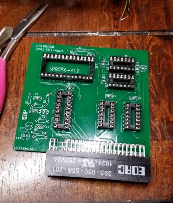
I received my boards
Now I just need to solve an annoying display problem before I can try them out

And a little MtM adapter because it seemed usedful
Re: This weekends projects
Posted: Sat Aug 29, 2020 7:32 am
by mcarlson_sb
Process pics:

- Socketed
Missed a GND trace

but it was an easy fix
Complete
Looking forward to testing it once I get my RAM issue figured out
Cheers,
Matthew
Re: This weekends projects
Posted: Sat Aug 29, 2020 10:04 am
by 1024MAK
It’s not proper without at least one bodge wire...

Looking good
 Mark
Mark


