Hi,
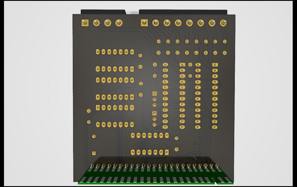
I plan to build a ZX81 card around the AN7225 chipset.
But i cant figure out the "\LDAC" process !
Can you help me, please.
AD7225 Datasheet:
https://www.analog.com/media/en/technic ... AD7225.pdf
My wiring diagram (POKE 0-7,value to set the output voltage= POKE 0,255 >> 5V to the 0 output channel)
8 Analog ouput card [AN7225]
Last edited by XavSnap on Thu Dec 07, 2023 8:41 pm, edited 1 time in total.
Xavier ...on the Facebook groupe : "Zx81 France"(fr)
Re: 8 Analog ouput card [AN7225]
I can't really help but inform you that the calculator routines of ZX81 ROM write to memory addresses 0 TO 5 which may confuse your device.
Also 7,8,9 are often used for paging ROM and RAM (at least in Germany) in ZX96, ZX97, ZX2000 etc.
Adresses above 16 should be safe to use.
Also 7,8,9 are often used for paging ROM and RAM (at least in Germany) in ZX96, ZX97, ZX2000 etc.
Adresses above 16 should be safe to use.
In theory, there is no difference between theory and practice. But, in practice, there is.
- 1024MAK
- Posts: 5118
- Joined: Mon Sep 26, 2011 10:56 am
- Location: Looking forward to summer in Somerset, UK...
Re: 8 Analog ouput card [AN7225]
This is what I understand from the datasheet:
The chip contains two sets of four registers.
The /WR control line and the two address inputs A0, A1 enable the processor to write new data into the relevant input register (one of four, one per DAC). This process will have no effect on the outputs if /LDAC is high.
This is because the second set of four registers supplies the DACs with their current data. This second set of registers will load the data from the input registers when /LDAC is pulsed, specifically on the rising edge.
This enables the processor to update all four input registers with new data, then pulse /LDAC so that all four outputs change simultaneously. This is what the datasheet refers to as double buffering.
Alternatively, if this is not needed, the /LDAC input can be tied low to 0V/GND. Then the second set of four registers that supplies the DACs with data will be transparent, that is, as soon as the processor updates the relevant input register, the DAC will respond immediately.
So either feed /LDAC from a second decoded address, or tie it low.
If feeding /LDAC from a second address, the software needs to write data to one or more input registers, then to update the outputs, write to the second decoded address (the data value is irrelevant). During this, /WR should be held high.
The same /LDAC signal can be shared between multiple DAC chips.
Mark
ZX81 Variations
ZX81 Chip Pin-outs
ZX81 Video Transistor Buffer Amp
Standby alert
There are four lights!
Step up to red alert. Sir, are you absolutely sure? It does mean changing the bulb
Looking forward to summer later in the year.
ZX81 Chip Pin-outs
ZX81 Video Transistor Buffer Amp
Standby alert
There are four lights!
Step up to red alert. Sir, are you absolutely sure? It does mean changing the bulb
Looking forward to summer later in the year.
Re: 8 Analog ouput card [AN7225]
Thanks Paul & Mark,
@Paul: Yes,better to force /ROMCS to deactivate the RAM/ROM process.
(ROMCS:high & RAMCS:high to get an ambiguous/undetermined stat)
The MEMOTCH HRG also use the 0-1fff RAM location.
@Mark: Thank, i had to primary set the DAC, and feed the DATAS in the buffer.
I had to use it with a single buffer, \LDAC to GND.
It was especially the simultaneous rising edge on the \WR & the \LDAC, my problem.
I planed to use two IRQs, one to change the DAC assignment, and one to feed the data bus.
Xavier ...on the Facebook groupe : "Zx81 France"(fr)
Re: 8 Analog ouput card [AN7225]
Wiring diagram updated:
Vss> GND
Vref on a terminal
\LDAC> GND or /WR (jumpers)
\ROMCS>high
Picture in the next message >>>
Vss> GND
Vref on a terminal
\LDAC> GND or /WR (jumpers)
\ROMCS>high
Picture in the next message >>>
Last edited by XavSnap on Fri Dec 08, 2023 8:14 am, edited 2 times in total.
Xavier ...on the Facebook groupe : "Zx81 France"(fr)
Re: 8 Analog ouput card [AN7225]
Last edited by XavSnap on Sat Dec 09, 2023 6:51 am, edited 2 times in total.
Xavier ...on the Facebook groupe : "Zx81 France"(fr)
- 1024MAK
- Posts: 5118
- Joined: Mon Sep 26, 2011 10:56 am
- Location: Looking forward to summer in Somerset, UK...
Re: 8 Analog ouput card [AN7225]
You need to be careful with the PCB layout. All the analogue chip pins, including the reference pins should be kept well clear of any digital signal lines. Better still if they are on separate sides of the board, or have ground/0V tracks between them. This is to reduce crosstalk, interference and noise appearing on the analogue lines. Hence you may want to change your board layout.
I see you have a diode going to the /ROMCS line.
I’m not sure you get the point made by Paul. Which is that some of the Sinclair ROM code actually writes to memory addresses between 0x0000 and 0x0005. Normally this doesn’t matter. But if you put hardware at these addresses, the ROM code will write garbage data to your hardware. Unless you are using a different ROM that doesn’t have this problem.
Mark
ZX81 Variations
ZX81 Chip Pin-outs
ZX81 Video Transistor Buffer Amp
Standby alert
There are four lights!
Step up to red alert. Sir, are you absolutely sure? It does mean changing the bulb
Looking forward to summer later in the year.
ZX81 Chip Pin-outs
ZX81 Video Transistor Buffer Amp
Standby alert
There are four lights!
Step up to red alert. Sir, are you absolutely sure? It does mean changing the bulb
Looking forward to summer later in the year.
Re: 8 Analog ouput card [AN7225]
Hi Mark,
Yes, it seem better now
Kicad project (wip temporary prototype)
http://zx81.ordi5.free.fr/brico/Carte_8Sana/
Yes, it seem better now
Kicad project (wip temporary prototype)
http://zx81.ordi5.free.fr/brico/Carte_8Sana/
Xavier ...on the Facebook groupe : "Zx81 France"(fr)