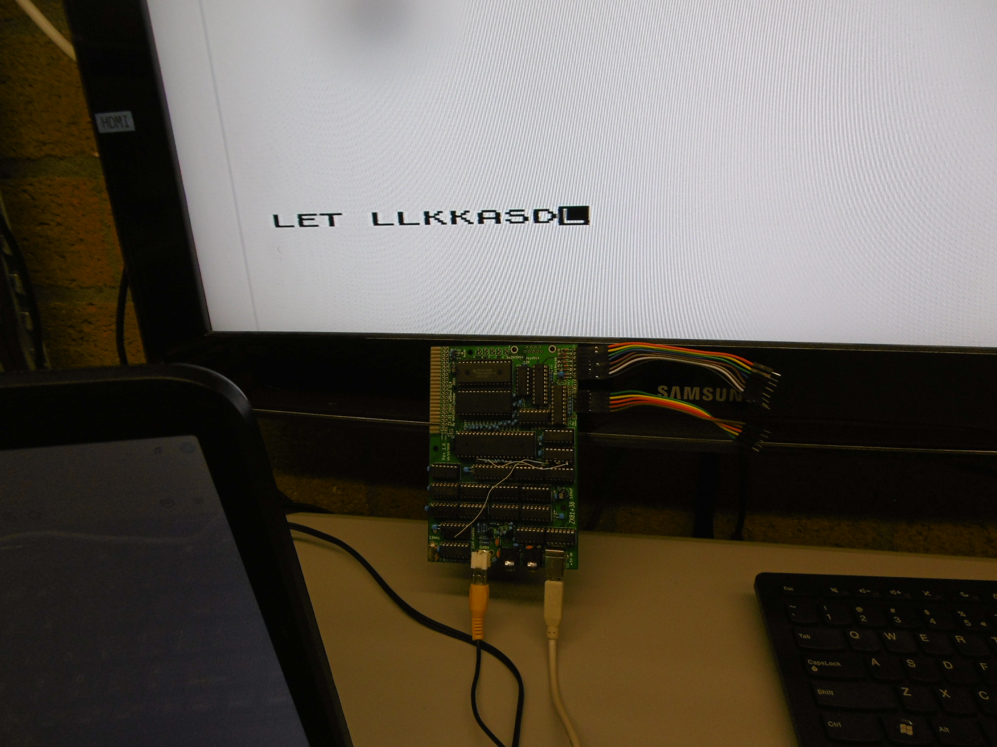
Going on the rev 1,6 schematic…jojo wrote: ↑Wed Dec 29, 2021 8:22 am hi forum ,
i found several pictures of build clones with a cat28c256 on it , but
how did you guys manage to get an cat28c256 working on this board ??
i know there is a track to be cut ( as indicated on the pcb ) , but what else needs to be done ?
patch wire 27 to 1 , but what about j10 ?? as indicated in the readme files
Pin 1 on a 28C256 is A14. Either leave the track intact and program the ROM image from address 0x4000 upwards (in the ‘top half’) in the 28C256. Or cut the PCB track and link pin 1 to 0V/GND (pin 14) and then you can program the ROM image from address 0x0000. Both these addresses are that of the 28C256 and programmer NOT the Z80 address.
You can connect pin 1 to the Z80 address line A14, but the system uses A14 for address decoding (see a ZX81 memory map) which restricts the amount of ROM to a maximum of 16kbytes between 0x0000 and 0x3FFF. So it does not gain you anything.
Pin 23 on a 28C256 is A11, so JP8 needs to be linked/jumpered to A11. This is the default position via a PCB track so should not need changing.
Pin 26 on a 28C256 is A13, so JP9 needs to be linked/jumpered to A13. This is the default position via a PCB track so should not need changing.
Pin 27 on a 28C256 is /WE so JP10 needs to be linked/jumpered to +5V. As the the default position via a PCB track is for 0V/GND, this needs changing. So very carefully cut the PCB track between the pins. Then solder a wire link across the other position, so that pin 27 connects to +5V.
JP1 needs to be set to the 16k position if your ROM image is 16kbytes. The default position via a PCB track is for an 8kbyte ROM image.
All the official ZX81 ROM images are 8kbytes in size.
Mark
Note: edited to make the situation with the selection jumpers clearer.